Symmetric
Symmetric Computer Systems (SCS) was funded by William Jolitz in 1982 in California/US. Their first system should have been the S/750, a powerful machine with bit mapped graphics. But the venture capitalist that did their series A asked for "something smaller", and they didn't believe in the bit mapped graphics, which was half the development cost.
So the S/750 was cut in half and became the S/375. The hope was to build the S/750 after the S/375. But the capitalist wanted other stuff - there were a lot of oddball derivatives of the S/375.
In August 2019 I got an email from William which told me the above details of the Symmetric story. Unfortunately his website is no longer accessible.
Symmetric 375
The Symmetric 375 was packaged in a nice case with a scope-type handle for carrying. It was built around the NS32016 CPU running at 10 MHz and used the FPU and the MMU. Main memory was 2 Mbytes, no wait states and no parity protection. Hard drive was 50 MByte minimum. The system software was a sort of Berkeley 4.2 . The price of the basic version was around $5000. Upgrades were available, for example a bigger hard disk drive. For $4000 more Ethernet hardware was included.
William wrote about the memory on the board:
"Not just 2MB - there are 8MB boards as well. They were costly because we could never get a good price on DRAM they required."
The system shown here is owned by Bernd K. Thank's to him for the photos.
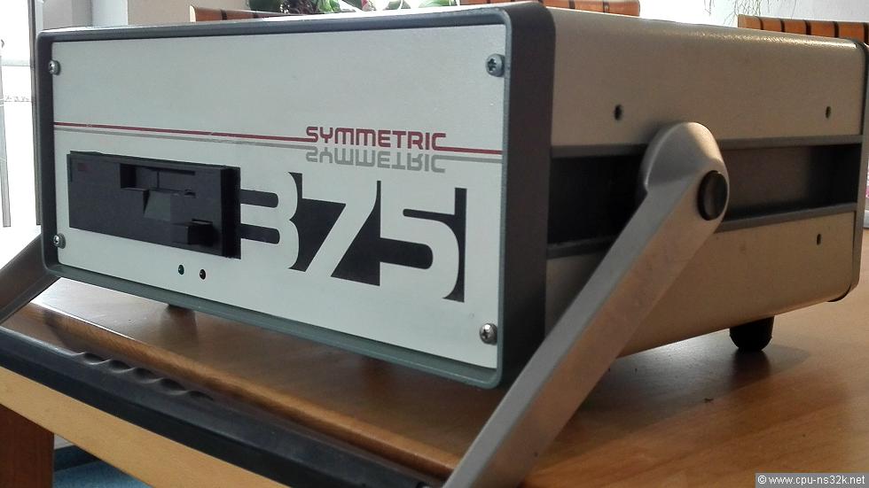
Fig. 1. The front side of the Symmetric 375 system.
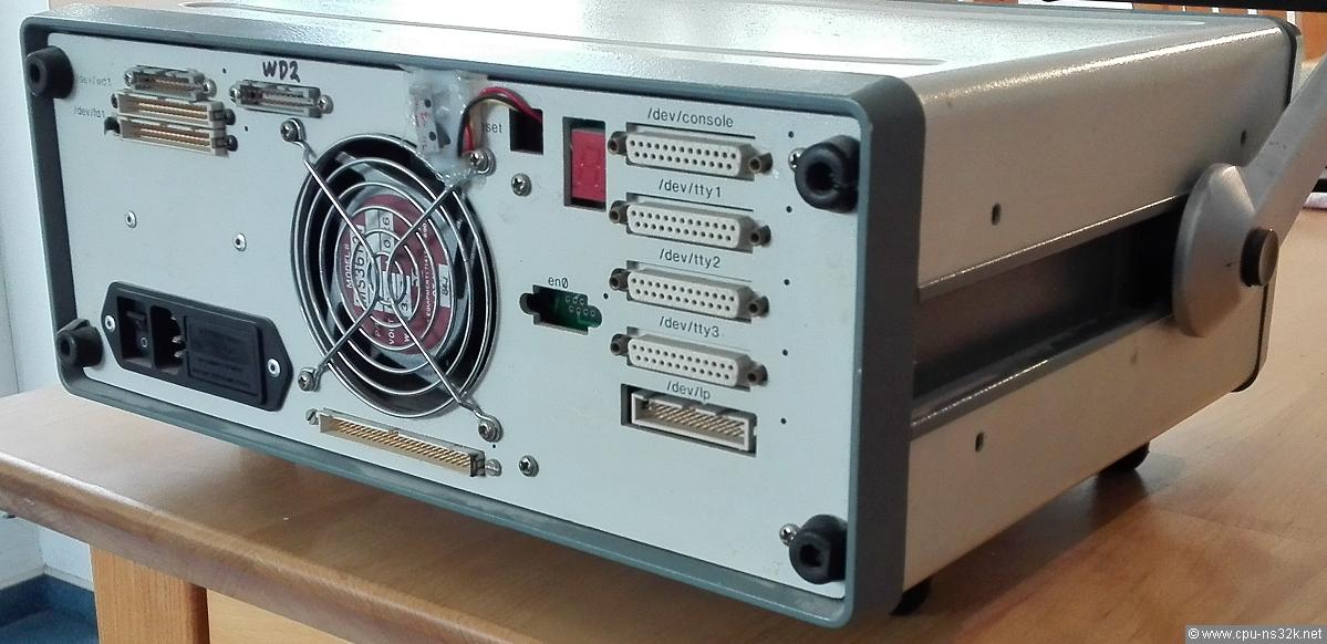
Fig. 2. The rear side of the Symmetric 375 system.
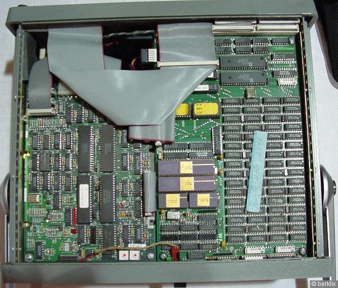
Fig. 3. A look inside shows that the system seems to be made of two boards (This photo is not made by Bernd).
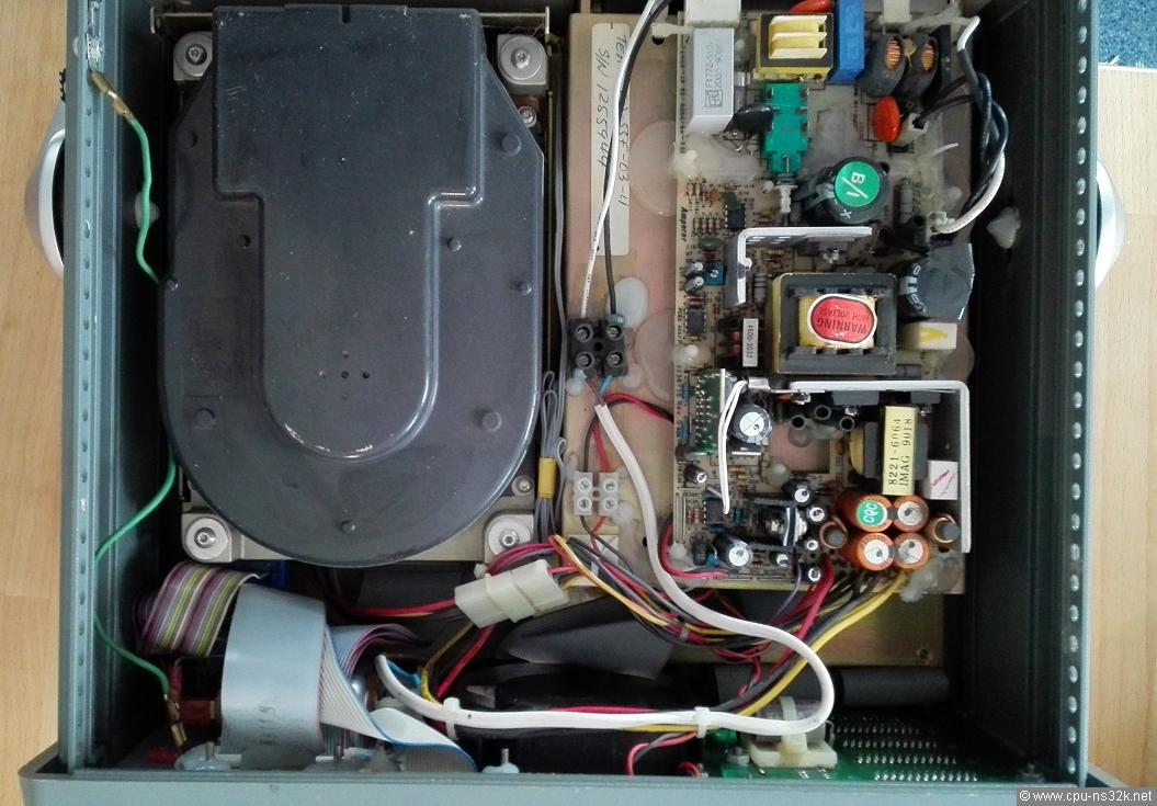
Fig. 4. The power supply and the hard disk drive of the Symmetric 375 system.
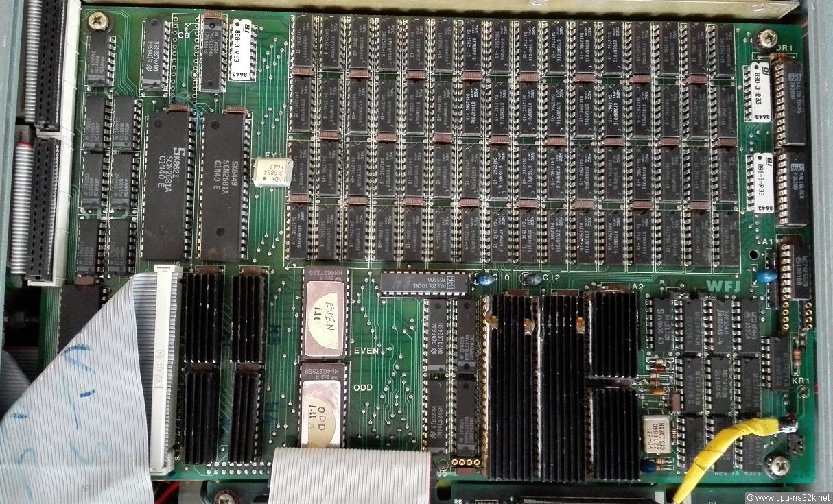
Fig. 5. This compute board uses heat sinks on the Series 32000 parts and on some other chips.
The heat sinks shown in Figure 5 are obviously needed because the Series 32000 chip set is overclocked. The quartz has a frequency of 22.118 MHz which will result in a system clock of 11.059 MHz. 22.118 MHz is used to generate baud rates because it is 9 * 128 * 19,200 Bauds.
Was the system already delivered with the faster frequency or did a user this upgrade?
The two SCN2681A are dual channel asynchronous receiver/transmitter devices. The WFJ on the PCB stands for William Jolitz.
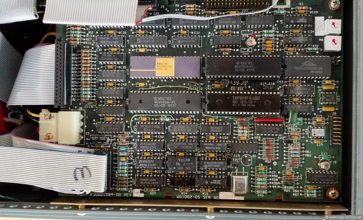
Fig. 6. The board shown is the WD1002-05 Winchester/Floppy Disk Controller from Western Digital.
It is not a bad idea to use devices from other vendors to shorten the time to market for the own development. This was obviously the case for the disk controller which was bought from Western Digital. The OEM manual of it can be found at bitsavers.org: Manual WD1002-05.
The chip named WD1015 is the "Control Processor Buffer Manager". Western Digital wrote about it that it is the heart of the control logic. But it seems to be only a programmed microcontroller instead of a custom design: the other name of the chip is TMP8049 which is an 8 bit microcontroller from Toshiba.
This chapter was last modified on 11 March 2020. Next chapter: Technos