Die Photos
It is always fascinating to see the die of a chip. During the 1980's the structures were clearly visible. Two layers of metal were placed on top of most chips. They served as interconnects between the thousands of transistors and delivered power, clock signals and all the many data signals. Today process technology is so advanced that you can not longer identify any details.
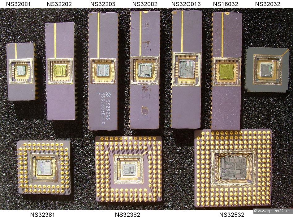
Fig. 1. Family portrait of Series 32000 members in ceramic package - ideal to see what is inside.
Some of the die photos presented here are the work of Pauli Rautakorpi from Finland. He is a highly skilled photographer with a passion for die photos. He gave me the permisson to show his Series 32000 die photos here. His really phantastic collection can be seen at wikimedia: Birdman86. He is always on the look for new chips which are not yet portrayed.
Pauli presents not only one photo of each die. There are different resolutions available. To ease the access I have set a link to the specific entry of his website behind the text of each of his photos.
Another "Thank You" goes to Herbert. He is now in retirement. If I get new chips in a plastic package it will be very difficult to get die photos...
NS16032/NS32016 (CPU)
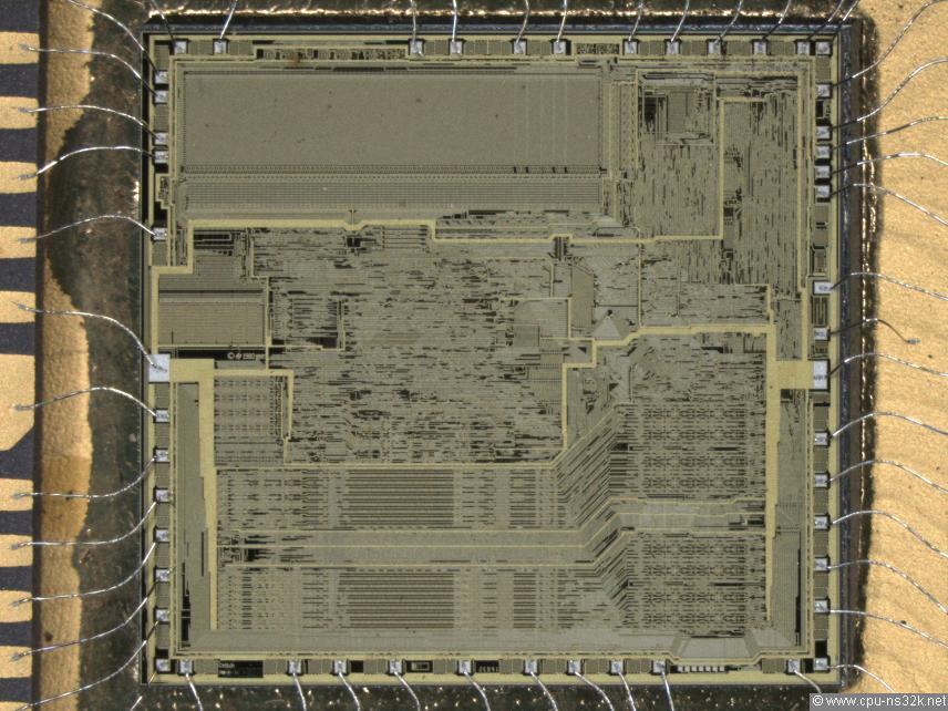
Fig. 2. The first NS16000 microprocessor: the NS16032.
The die in Figure 2 is possibly coated with a polymide to protect its surface. Therefore the color is not metallic like the other dies shown. The bond wires seem not to be made of gold as usual. At the top is the microcode ROM. The size of the ROM is 1300 words by 18 bits according to a conference paper at the ISSCC 81. 127 words are used for self test routines. At the bottom is the datapath. The same die photo with 3 times higher resolution can be downloaded. Then you can see a date and the chip name which is still 16032. Die size is around 7.5 mm * 7.3 mm = 54.75 mm².
NS16032 die in high resolution
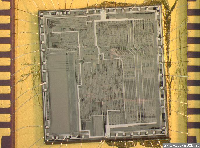
Fig. 3/4. What do you expect to find under the lid with the marking of the left photo? Surprise, surprise ... it is an NS16032 shown in the right photo.
The dies in Figure 2 and 4 are obviously identical. But they are different in very small details, see Figure 5 and 6. The word ISRAEL is not found in Figure 2 in the middle of the lower edge. SLC is not found in Figure 2 in the middle of the left edge. Maybe the die in Figure 4 was a very early internal version. This could be also the reason for the strange marking without the complete product name, National Semiconductor logo and stepping code. I would have been not interested in the chip if I didn't got the strong advice that this is a NS16000 device ...
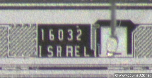
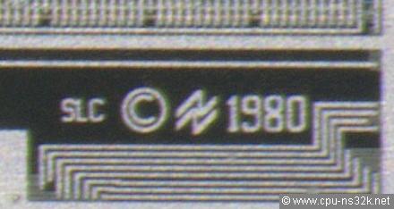
Fig. 5/6. Two enlarged areas of the die in Figure 4 showing differences to the die in Figure 2.
The meaning of ISRAEL is obvious which is not true for SLC. I got the info that it means the town Salt Lake City in the US. It was the location of the fab of National Semiconductor where the NS16032 was manufactured.
The next photo shows the die of Figure 4 in a way which is not natural for a human being: black is becoming white. This photo is made with equipment of a semiconductor company showing details which are otherwise not visible. Thank's to Herbert!
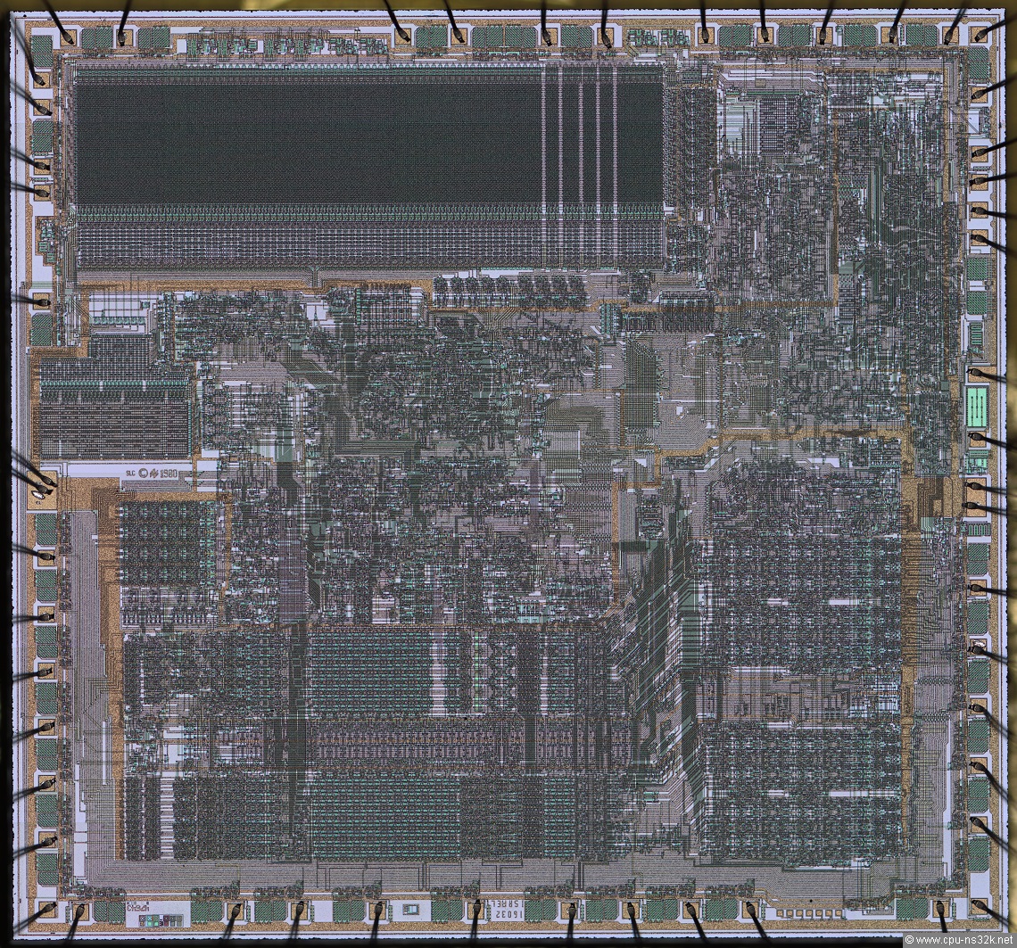
Fig. 7. This is the best photo of NS16032 I have ever seen!
If someone is alreay impressed by the photo shown above he or she should download the larger version of it: NS16032 die in super resolution.
NS32032 (CPU)
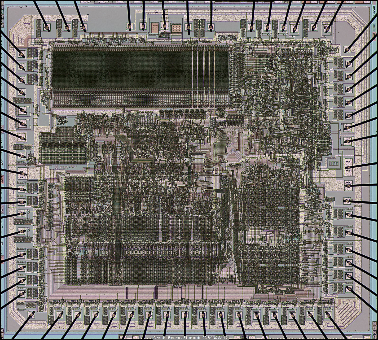
Fig. 8. The first Series 32000 microprocessor with an external 32-bit data bus: the NS32032. Die size is 6.7 * 6.0 = 40.2 mm².
If you compare Figure 2 and 8 you see that the NS32032 is the big brother of the NS32016. From a programmer point of view the chips behave identical. But the architecture of the NS32032 must be slightly different because of the 32-bit data bus. In the middle of the right edge there are two power pads. You may think that one pad is for VCC and the other pad is for GND. But the upper pad is GNDB for the buffer supply and the lower pad is GNDL for the internal logic. This separation is done to avoid disturbances from the fast switching buffers. The disadvantage of this solution is the risk of ESD damage during handling of the chips.
From an electrical point of view it would be better to use a second wire (double bonding) on the GNDB pad.
The date code of the device is S9206AB. Together with the small die size I assume that this device was built in 2.8 μm NMOS technology.
NS32C016 (CPU)
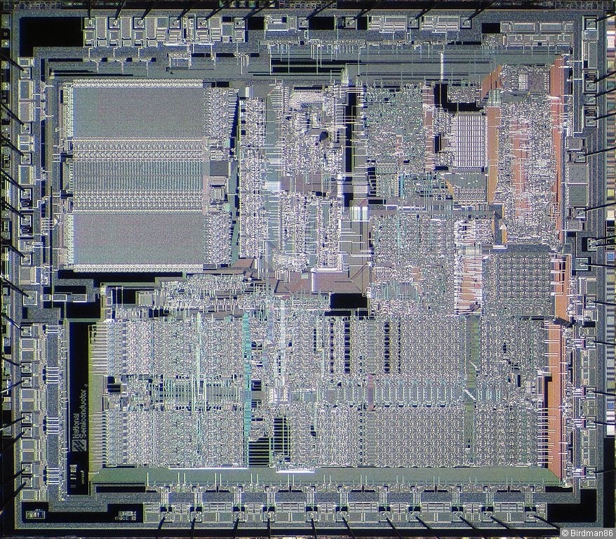
Fig. 9. The first CMOS Series 32000 microprocessor: the NS32C016. Die size is 9.2 * 8.0 = 73.6 mm². (Birdman86:NS32C016)
The CMOS NS32C016 is obviously the successor of the NMOS NS32016 as can be seen in their die photos. The big long microcode ROM of the NS32016 changed its shape to a square part of the NS32C016 die. This gave room for some shiftings. For example the little memory (ROM ?) at the middle of the left edge of NS32016 moved to the upper right corner of NS32C016. National Semiconductor seems to have rejected functional changes to the newer NS32C016 to avoid any risks. Clock-by-clock both CPUs are identical.
The large die size can only be explained with the 3 μm feature size of the used CMOS technology. Please note the large company logo and the name of the company in the lower left corner. This kind of marking a die can be found on the NS32382 MMU too.
NS32332 (CPU)
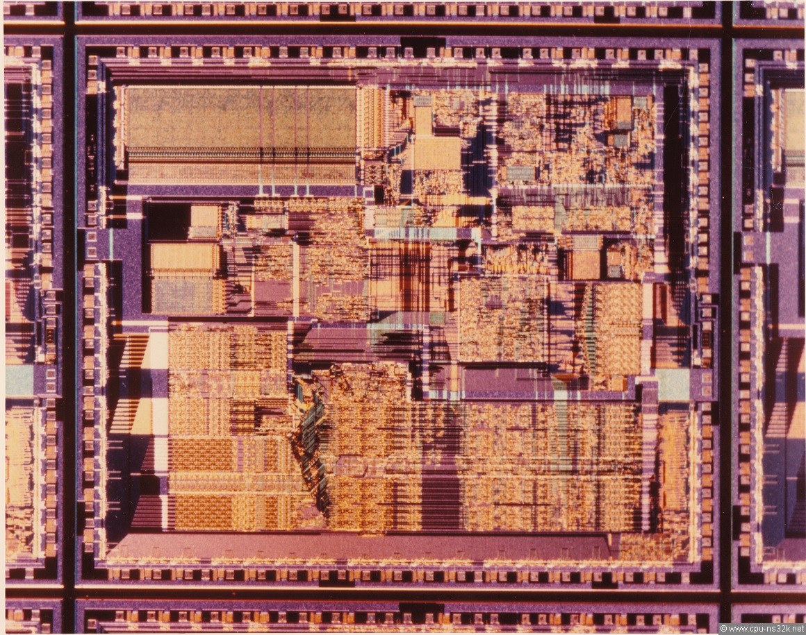
Fig. 10. The second generation Series 32000 microprocessor: the NS32332. Die size is 10.1 * 8.7 = 87.87 mm².
The NS32332 was the first CPU of Series 32000 which had an address space of 4 Gbyte. The external address bus was 32 bits wide and was multiplexed with the 32 bits wide data bus. This CPU would have been a much better device for all the companies who have built multiprocessor systems based on the NS32032. This CPU could only address 16 Mbytes. But the NS32332 appeared to late for this market.
David Rand sent me the photo. It shows the die being part of a wafer! Unfortunately David has only the photo and not the wafer ...
The layout of the NS32332 die looks similar to the NS32032 in Figure 8. For example the ROM in the upper left corner is nearly identical in both dies. The outer metal ring delivers GND for the I/O pads. In the NS32332 the ring is cut into 6 segments. Each of the four segments in the lower half of the die has 8 I/O pads and one GND pad. These four segments make the 32-bit address/data bus. The double pads at the left and right edge deliver VCC resp. GND for the internal logic.
The distance die-to-die on the wafer is around 150 μm. There are no test structures visible between the dies. This is also true for the wafer in Figure 19. National Semiconductor didn't waste any valuable space on the wafer.
New photo of NS32332
Antoine made a photo of an NS32332 in 2023 which has some test structures at the chip edges: NS32332 die. It is difficult to find some differences between Figure 10 and the new photo. For example the two pad positions at the lower left side of the microcode ROM are different.
NS32532 (CPU)
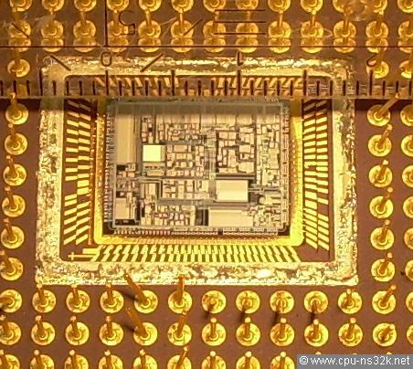
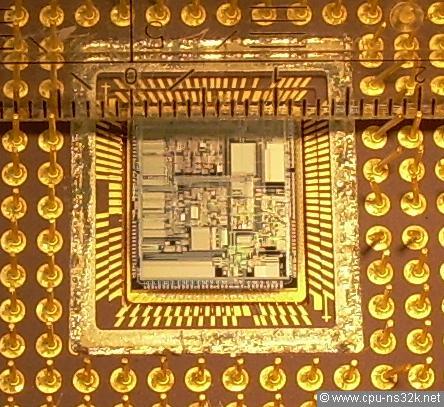
Fig. 11/12. How big is the NS32532?
The answer to the above question is : 11.5 mm * 14 mm = 161 mm². A huge die even for today! The wafer size in the 80's was growing from 100 mm (4 inches) to 150 mm (6 inches). Today it is 300 mm (12 inches). I don't know what National Semiconductor was using but even if you use 150 mm wafers you get less than 100 dies. The area of a 150 mm wafer is 17,670 mm² but the wafer is round and the dies are square. Therefore you loose dies at the edge. Programs are used to optimize the number of dies per wafer. And the next problem is defect density. This number represents the qualtity of the wafer material measured in crystal errors per square centimeter. If you have a defect density of 10 errors/cm² the probability that one of them will hit a transistor in the NS32532 is high. And then you have a defect die which you can not sell.
Since I saw for the first time a die of the NS32532 I was wondering where were the different functions located. For me it was not clear, what was a data ram, a tag ram, a microcode rom or an associative memory. In August 2017 I got a copy of an article of 1989 that answered just these questions. The next Figure shows the die together with an identification of the particular functions.
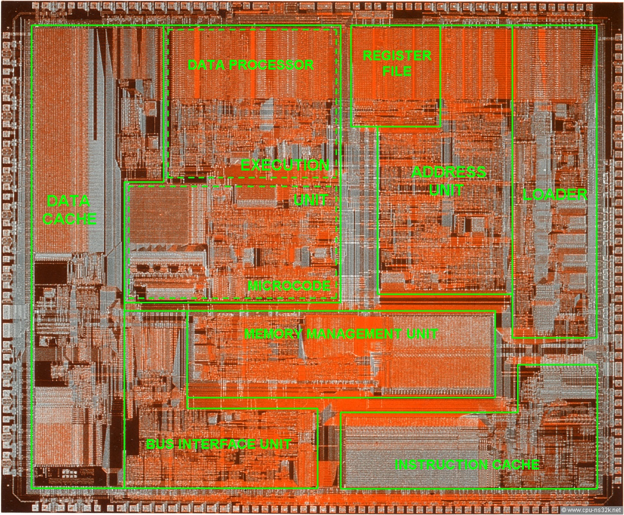
Fig. 13. The building blocks of the NS32532 and their location on the die.
On the left side of the block called microcode inside the execution unit is the microcode ROM. Its size is 1K words by 44 bits.
Fig. 14. The designers of NS32532 placed their names on the first silicon.
Figure 14 can be found in Figure 13 in the lower left corner. Later the designers were not allowed to do so again...
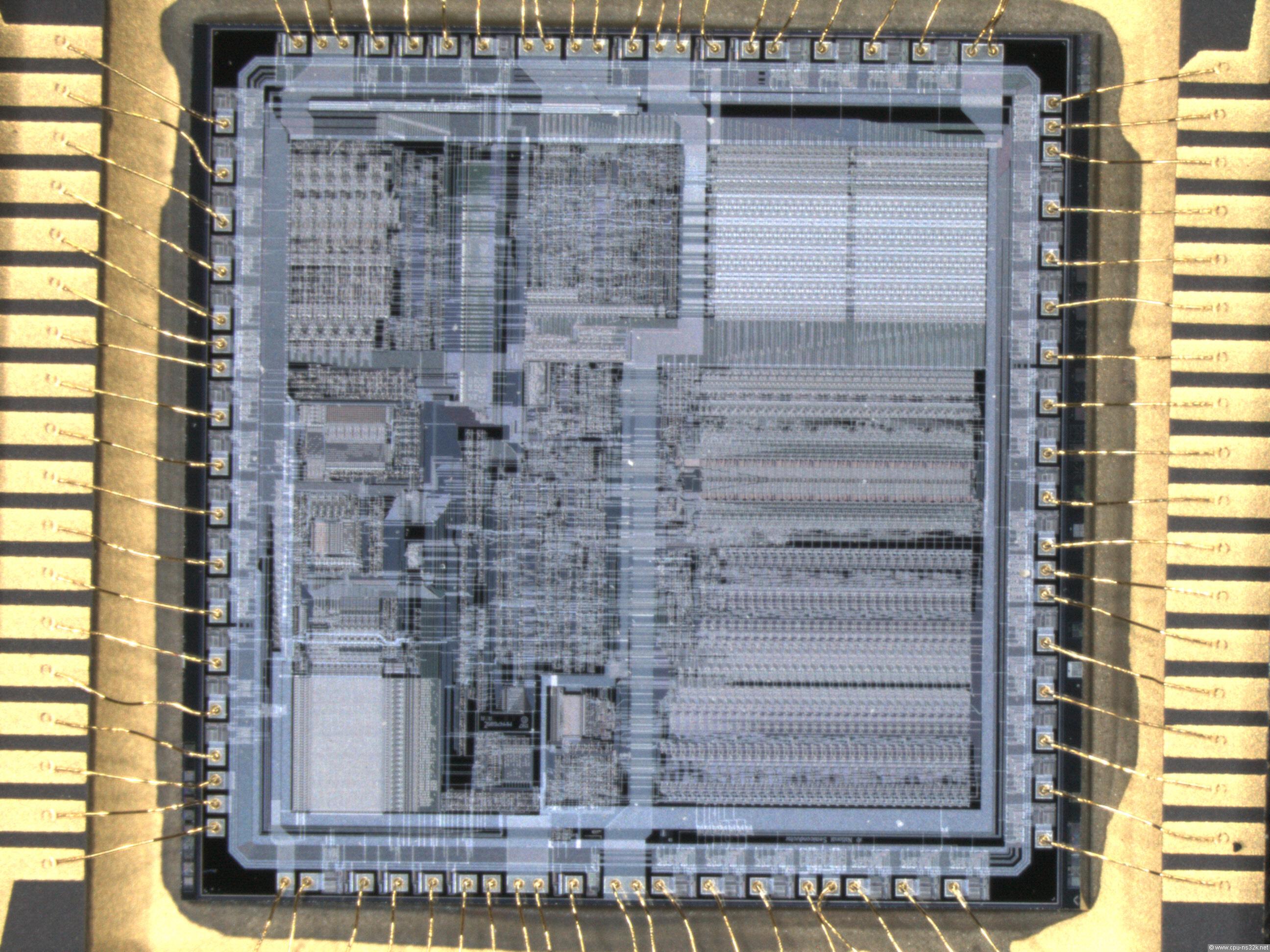
And now comes the absolut highlight : a die photo of the NS32532 with 10,560 by 8,560 pixel! This photo is taken by a high quality optical tool from the semiconductor industry. The file size is 39 MB. Download and enjoy!
NS32532 die in very high resolution
Obviously the die in Figure 13 and the one in high resolution are different. Figure 13 shows the die of the first silicon which was fabricated in 1.5 μm CMOS technology. The die in high resolution is a production part and used a 1.25 μm CMOS process. Initial parts run at 20 MHz and the shrinked parts could be rated at 25 and 30 MHz.
It is interesting to note that the production die has some empty area. The reason is that both dies are of the same size. The engineers shrinked only the logic transistors and kept the die area the same because they needed the long edges for the many pads. The semiconductor industry calls such a design "pad-limited". Another advantage is that the wafer test equipment can be reused.
Swordfish (CPU)
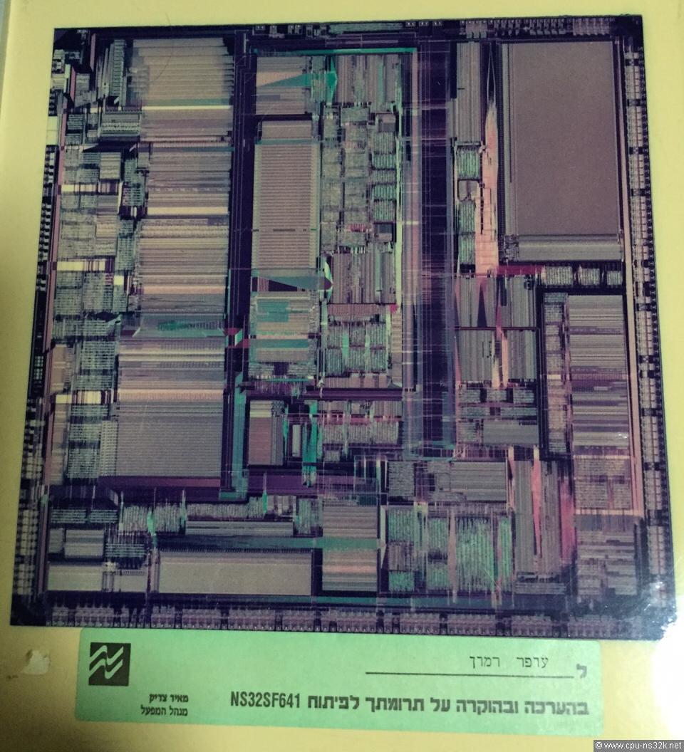
Fig. 15. The next step of Series 32000: the NS32SF641
The photo in Figure 15 shows according to the text the NS32SF641. This chip has 1.1 million transistors and is much more complex than the NS32532. For the first time the FPU was integrated. The technology used was 0.8 μm CMOS. In a conference paper it is written that the die size is 13 mm * 13 mm = 169 mm². Compare this design to the die of the NS32016 and you get an impression of the progress in the semiconductor industry within one decade. In 2020 such a chip would fit in less than one square millimeter...
The CMOS process of Swordfish had only two layers of metal. To build such a complex chip with only two layers is definitly a disadvantage. Using a third layer of metal would shrink the die size significantly.
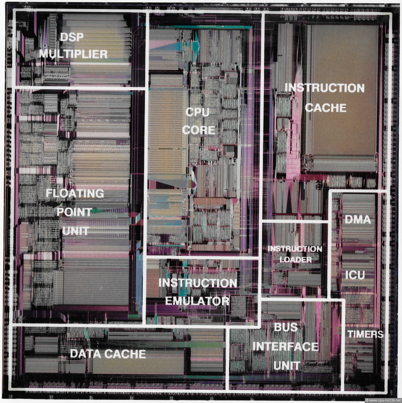
Fig. 16. The modules of Swordfish.
What is called the instruction emulator was intended to keep Swordfish's instruction set compatible to earlier Series 32000 processors. Later this unit translated only some special instuctions of Swordfish to a series of RISC instructions.
The size of the instruction cache is 4 kByte. The size of the data cache is 1 kByte. Swordfish contains no MMU.
Fig. 17. Swordfish in its 223 pin PGA package.
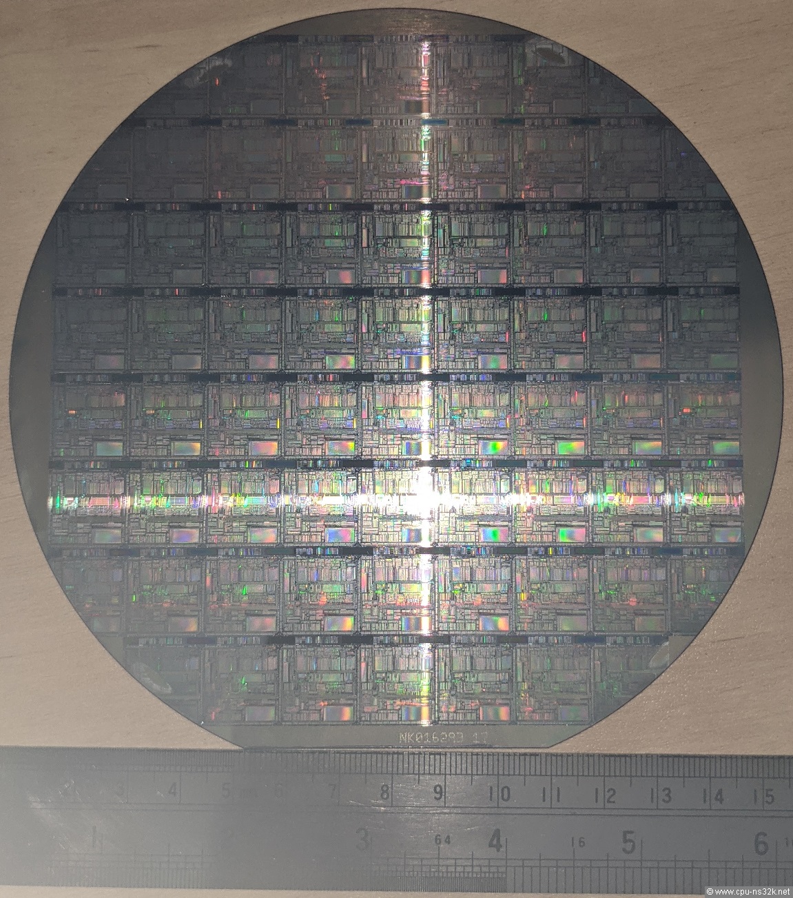
Fig. 18. The 6 inch wafer of Swordfish shows only 56 potentially good chips! This is no good news for the price of Swordfish.
Maybe two more chips in the third row from the top are available. But it seems that their corners are not fully processed. Some area could have been saved if the horizontal test structures between Swordfish dies were made smaller. Anyhow chips near the edge of a wafer see often a process problem.
I doubt that the published die size of 13 * 13 mm square is correct. Then 10 dies would fit in the row at the center. The real die size is nearly 15 * 15 mm square.
Maybe there was a plan to shrink the die...
NS32CG16 (CPU)
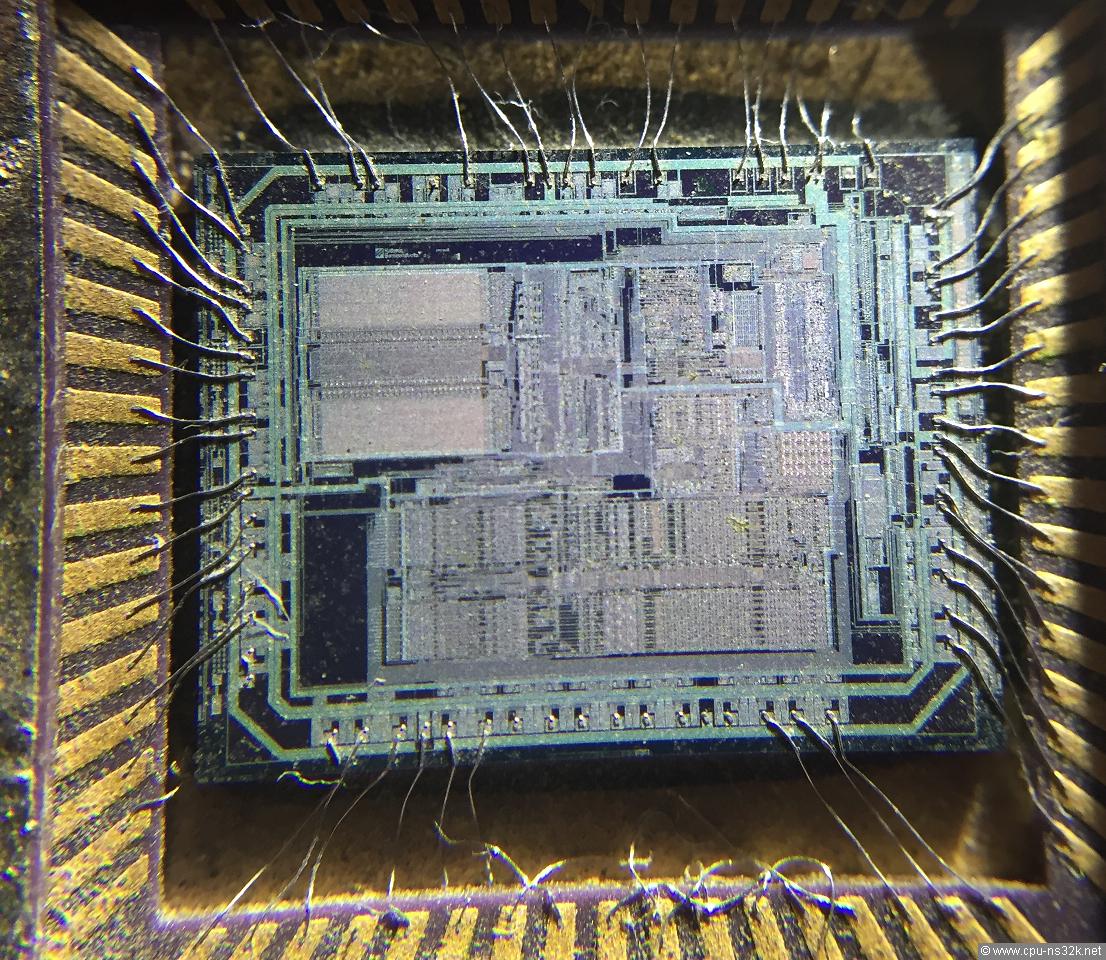
Fig. 19. The first Embedded Processor of Series 32000: the NS32CG16. Die size is 9.9 * 7.6 = 75.24 mm².
David Rand sent me the photo of his NS32CG16 device in September 2016. This chip must be the very first silicon of the NS32CG16 because of the large and complex test structures at the left and right edge. Normally simple and small test structures like ring oscillators are used for process monitoring in the fab. But on this device some people wanted to learn more ...
The core of the NS32CG16 is an unmodified NS32C016. The size of the microcode ROM was not changed because the new graphics instructions replaced the instructions for the MMU. At the right edge some additional structures are placed inside the pad ring. I guess that most of it is used for the block GRAPHICS SUPPORT LOGIC which is shown in the block diagram on page 1 of the NS32CG16 datasheet. Part of the structure must be the integrated functionality of the NS32201 TCU.
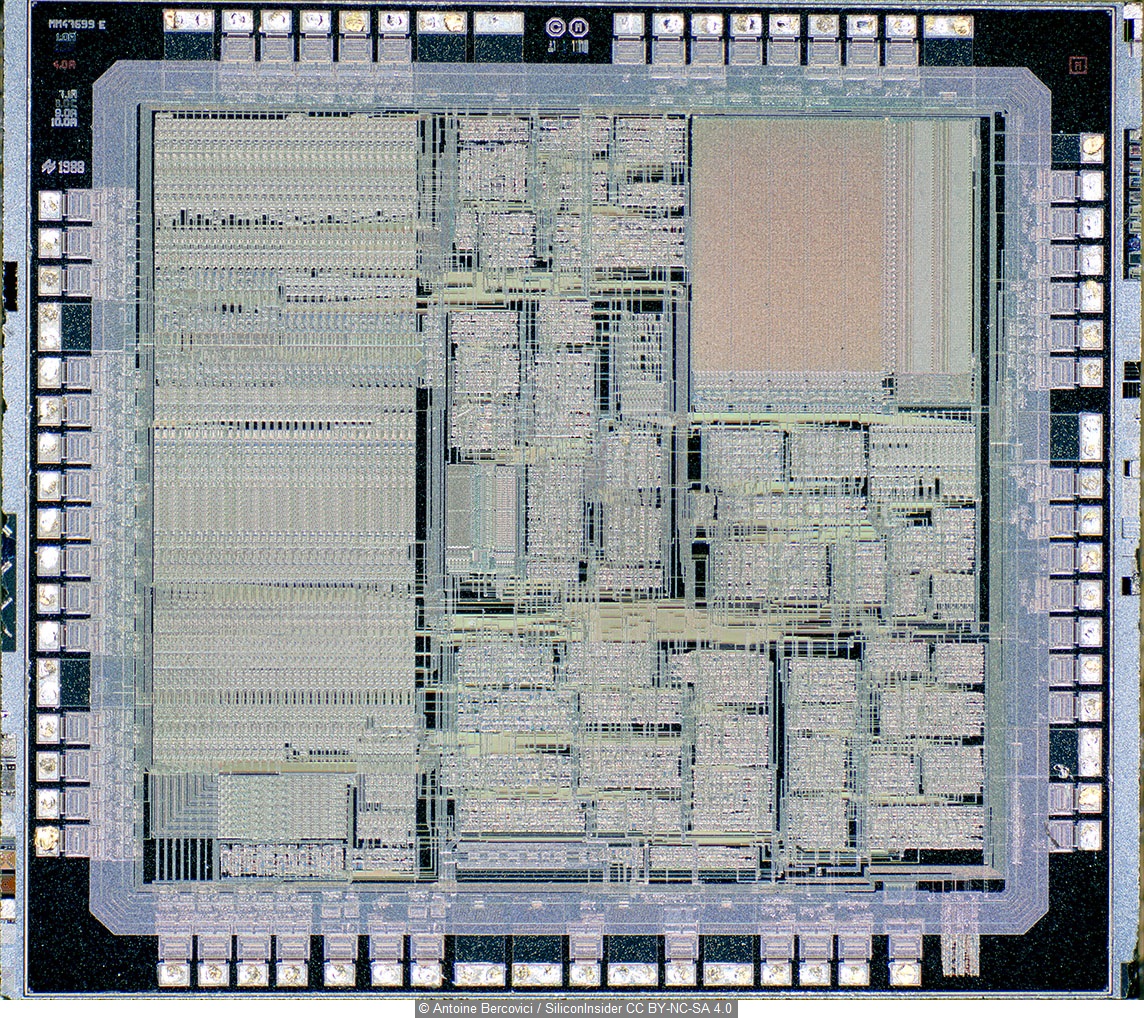
Fig. 20. This NS32CG16 is a production device with an optimized structure. Die size is 5.09 * 5.57 = 28.35 mm².
NS32CG160 (CPU)
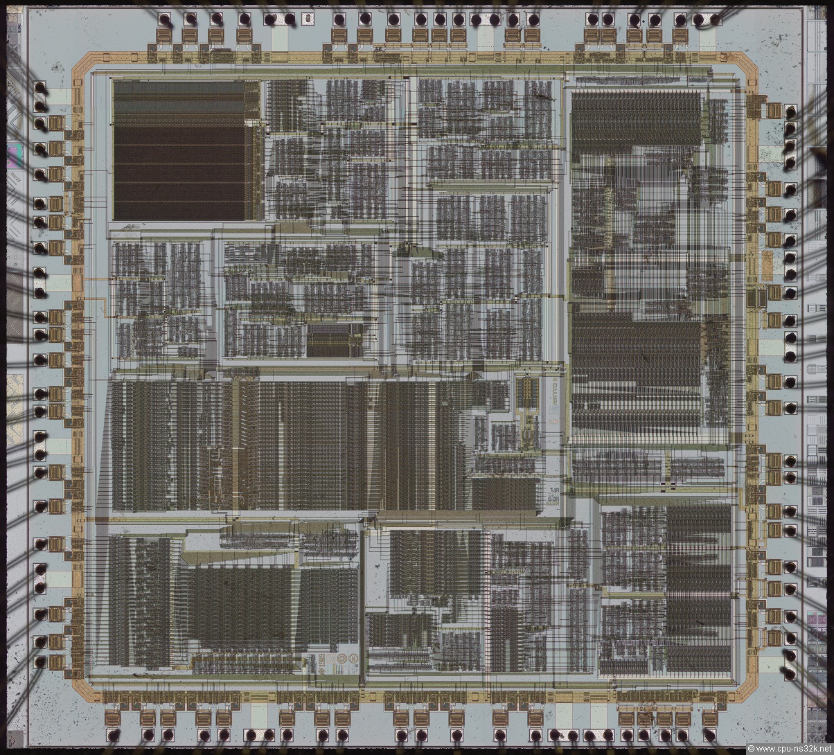
Fig. 21. The successor of the NS32CG16: the NS32CG160. Die size is 8 * 7.5 = 60 mm².
The NS32CG160 was one of the last Series 32000 designs. It was implemented in 0.8 μm CMOS. The CPU core takes the upper left area. The peripherals are placed at the right and at the bottom side of the die. Once again the IO structure has been changed. The year of the design was 1989. The number can be found in the lower middle of the die.
The design is not very compact. One of the reasons was that only two layers of metal were available for wiring. The situation changed dramatically when technological advancements allowed a third metal layer. To my knowledge there was never a Series 32000 device done in three metal layer.
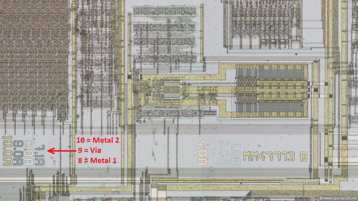
Fig. 22. An enhanced view of an area near the center of the die showing the clock generator. This view is rotated by 90 degree.
I didn't find the product name on the die. Only the internal design name MM47713 was placed in the metal 2 layer. The "B" can be the design step. Metal 2 is the top most layer of the used technology. The number 10 for metal 2 can be a hint to the total number of masks for this process. Both metal layers were made of aluminium. The layer 7, which should be the contact layer to the gates and diffusions, has a subversion number of 1. Maybe the microcode ROM content is defined in this layer.
The wiring between the blocks of logic has been done automatically. Although the results were always not perfect from an engineering point of view, it saved a lot of time. And time is money!
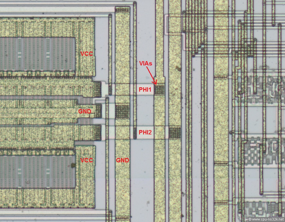
Fig. 23. A more enhanced view of the output of the clock generator showing the big transistors on the left side driving PHI1 and PHI2 at high speed.
In Figure 23 the connections between metal 2 and metal 1 are visible as small dots. Each dot is a via, which is a hole in the isolating oxide filled with aluminium. Due to technical reasons all vias have the same size. Even if the width of the metal allows for a big hole an array of vias is used.
The external clock signal has twice the frequency of the CPU clock. The clock generator shown in Figure 22 and 23 produces two signals at the CPU frequency. PHI1 is high when PHI2 is low and vice-versa. This is called a two-phase clock system. It is placed in a loop around the whole logic. Due to its limitations this clocking schema was later replaced by the clock tree.
I don't know how National Semiconductor named the clocks. I choosed the names PHI1 and PHI2 by chance. VCC and GND can be identified by following the wires to the pads and look for the names in the data sheet.
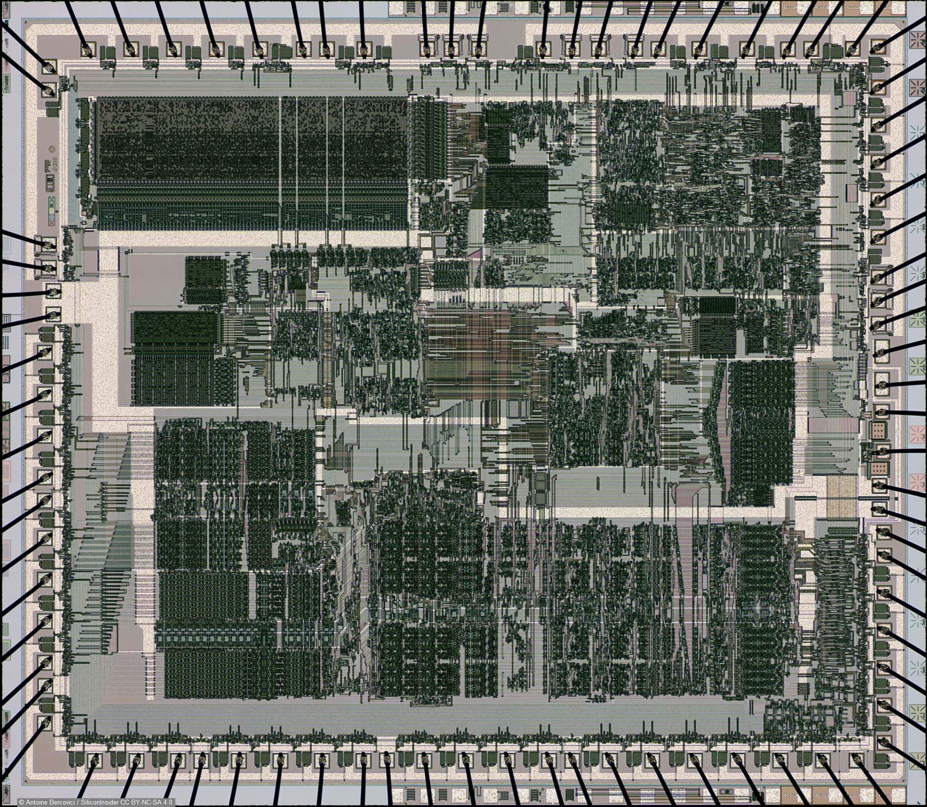
NS32GX32 (CPU)
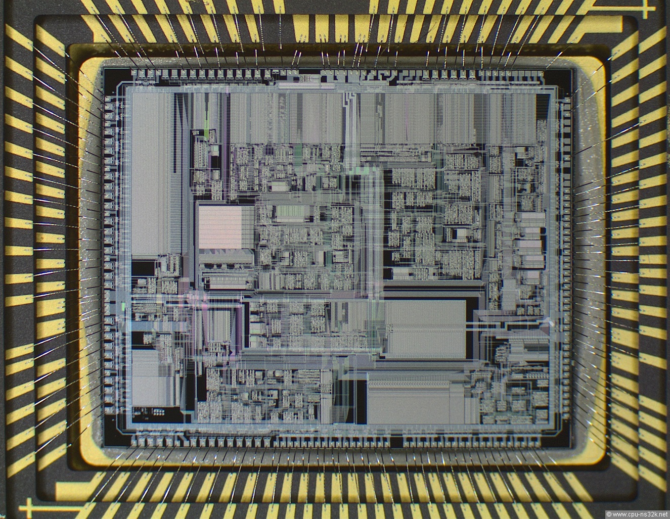
Fig. 24. Surprise, surprise: the die of the NS32GX32 CPU looks like the NS32532 CPU. Yes, it is the same die, but the MMU is not fully functional. Good trick to make money with a broken die...
NS32GX32A (CPU)
A long time I speculated about the differences between NS32GX32 and NS32GX32A. One theory was that the chip uses a newer technology. In December 2019 the X-ray image in Figure 25 confirmed this assumption: the die size of NS32GX32A is much smaller.
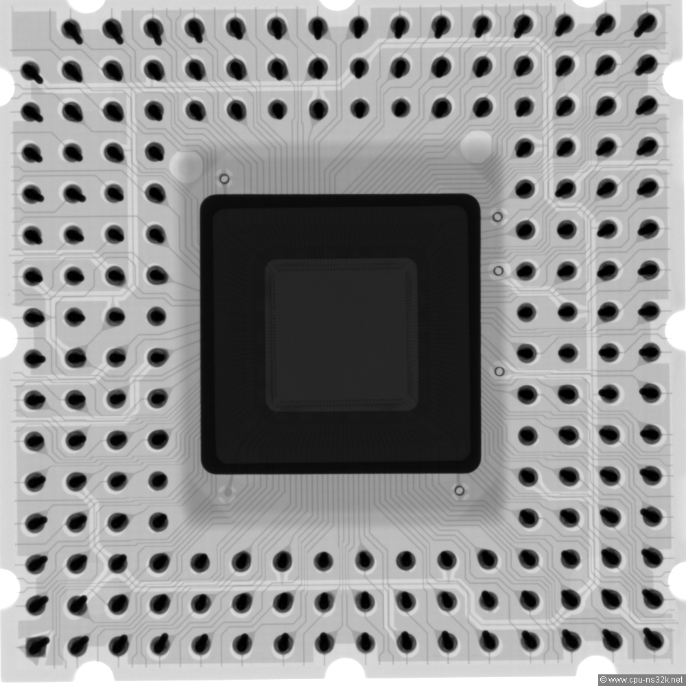
Fig. 25. The high quality X-ray image of the plastic package of the NS32GX32A shows even the bond wires between the die and the carrier.
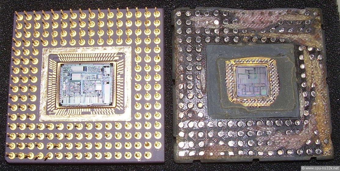
Fig. 26. A direct comparison of the NS32GX32 left and the "A" version right. Brute force was necessary to open the plastic package. Pin A1 is in the lower left corners.
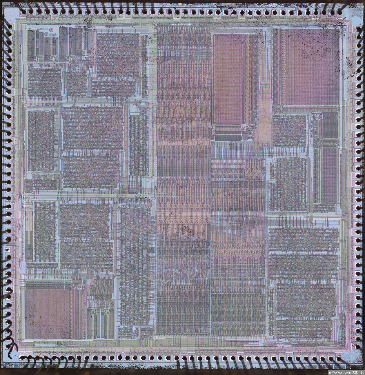
Fig. 27. The die size of the shrinked version is 9 mm * 9 mm = 81 mm² which is about half the size of the NS32GX32. The design was done in 1991.
Normally smaller technologies result in faster chips. But the NS32GX32A got the same speed selections like its predecessor. Now the design is obviously pad-limited.
I think that the 1 kByte data cache is in the upper right corner. Below must be the TAG RAM. The instruction cache of 512 Byte is on the left side of the data cache. These blocks should have 32 bits wide busses to the pads. The memory block in the lower left corner must be the microcode ROM.
Fig. 28. A nice view of another NS32GX32A not being destroyed but not finally processed.
NS16081/NS32081 (FPU)
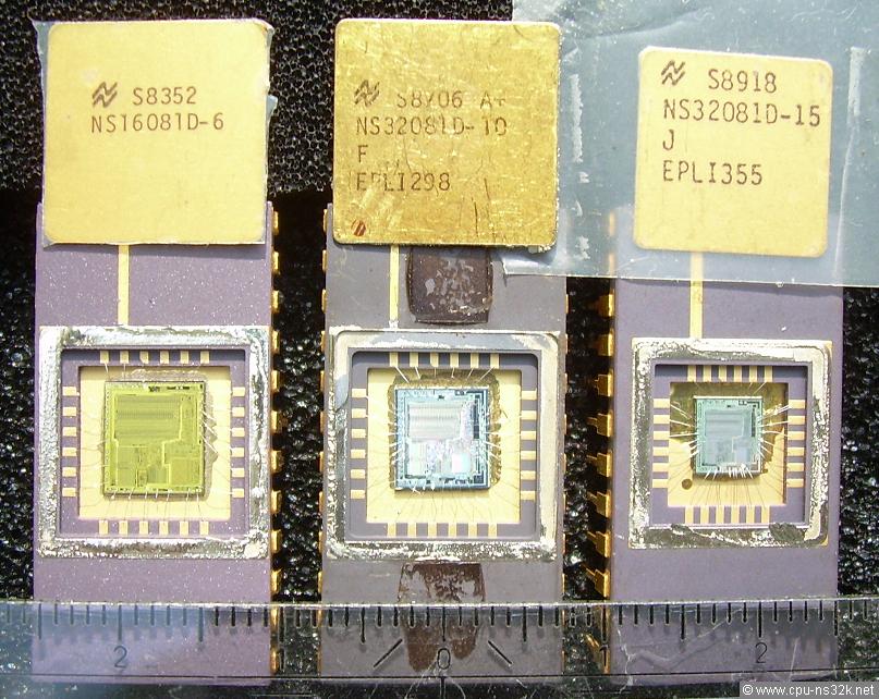
Fig. 29. The first Series 32000 FPU NS16081 and the later versions of NS32081 in comparison.
The NS32081 has a more compact layout compared to the NS16081. The die size of the NS16081 is around 7.0 mm * 6.4 mm = 44.8 mm². The die size of the NS32081D-10 is around 6.2 mm * 5.9 mm = 36.58 mm². The die size of the NS32081D-15 is around 4.8 mm * 4.5 mm = 21.6 mm². A smaller die has lower production costs.
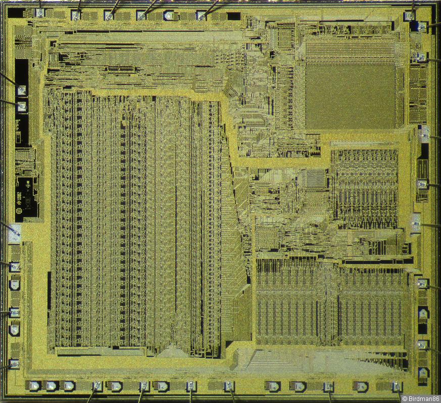
Fig. 30. A closer look at the NS16081 FPU. Die size is 7.0 * 6.4 = 44.8 mm². (Birdman86:NS16081)
The datapath is located in the left half of the die. The 8 * 32 bits register file of the FPU is placed in the lower right corner. A ROM is placed in the upper right corner. The purpose of it is not clear to me.
On the left edge there are 7 bond wires. The one in the middle is not going to a pad but is connected to the cavity of the package. It connects the on-chip back-bias generator to the backside of the die. Maybe someone remembers the -5V pin of early digital NMOS chips. These pins could be eliminated with the voltage generator placed on-chip. Modern CMOS technology does not require back-bias.
The NS16081 in Figure 30 has 13 additional pads for testing. They can be identified because there is no bond wire attached to them. The purpose of test pads can be different. They may help to shorten test time. This maybe true for the FPU because this device has too little ordinary pads. Test time depends on the amount of data to be written into and to be read from a device. More pads means more bandwidth. Or they are used for parametric testing to find speed critical paths.
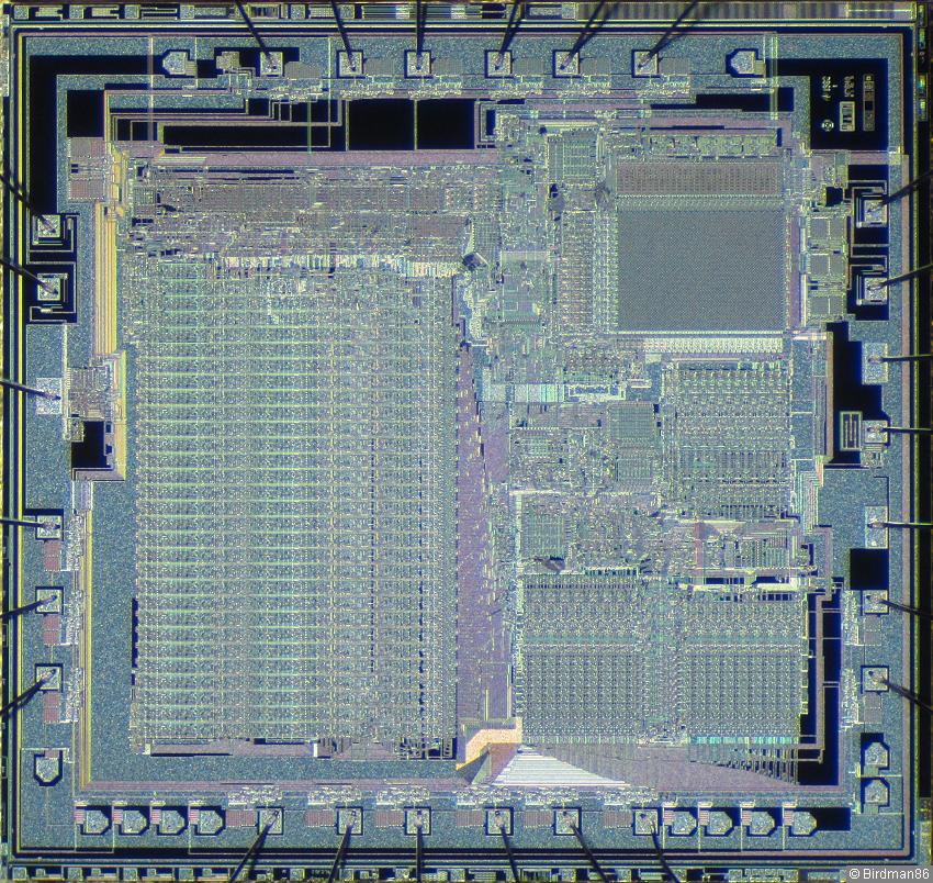
Fig. 31. A closer look at the NS32081 FPU. Interesting to note the different colour of the dies. Die size is 6.2 * 5.9 = 36.58 mm². (Birdman86:NS32081)
The NS32081 in Figure 31 has the same number of test pads. But their locations have changed.
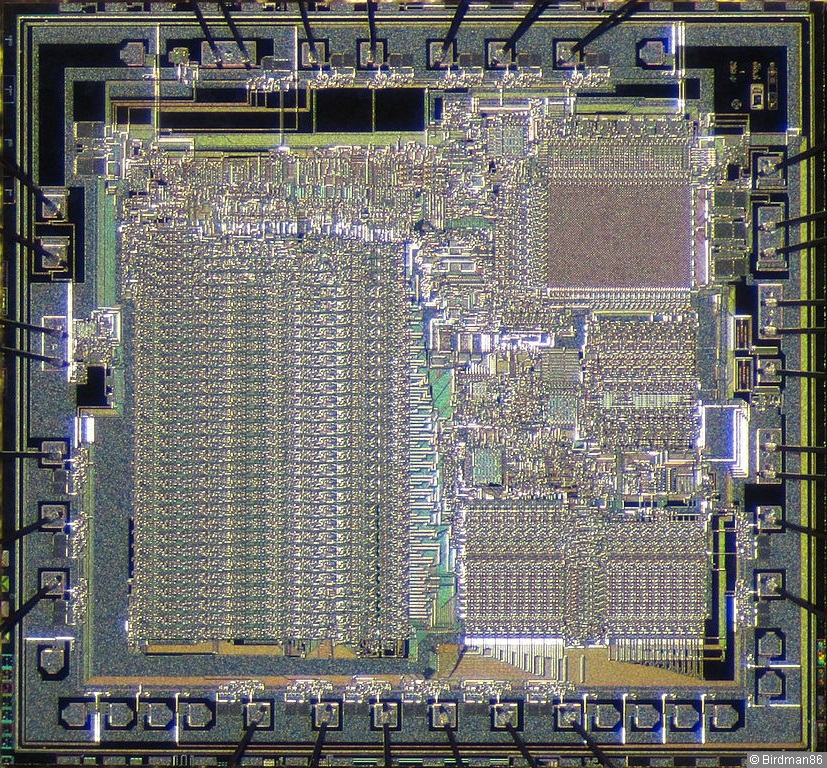
Fig. 32. The NS32081 FPU in 2.8 μm technology. Die size is 4.8 * 4.5 = 21.6 mm². ( Birdman86:NS32081 2.8 μm)
The NS32081 FPU in Figure 32 was built in 2.8 μm technology to achieve 15 MHz clock frequency. This was necessary to support the NS32332 CPU. In a smaller technology the pad size can not be shrinked in the same ratio. This is because bonding equipment is changed far less often then technology equipment. If you compare Figure 31 to Figure 32 you will notice a smaller pad distance. Surprisingly the newer FPU in Figure 32 has five pads with double bonding whereas the FPU in Figure 31 has none. Some of them are even used for signal pads: /SPC on the top edge and CLK at the top of the three double bonds on the right edge.
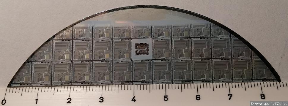
Fig. 33. A wafer full of NS16081.
In November 2015 I got my first photo of a Series 32000 wafer - see Figure 33. Unfortunately the wafer was broken. But I'm sure that somewhere on this planet a complete wafer exists.
The wafer in Figure 33 has a diameter of 10 cm or 4 inch. This wafer size was the standard for all NMOS products of Series 32000. Around 150 dies of NS16081 could be placed on it.
In August 2016 I got two NS32081 FPUs from John with a very unusual date code of S0925AD. I was very curious to see the die inside. Due to the plastic package I needed some professional help - thank's again to Herbert!
The analysis showed a die which is the newest version of the NS32081 FPU in 2.8 μm technology, see Figure 32. The reason for the date code of 2009 remains unknown.
Fig. 34. Acid is needed to free the die inside a plastic package. In this case the acid was carefully applied to keep most of the package.
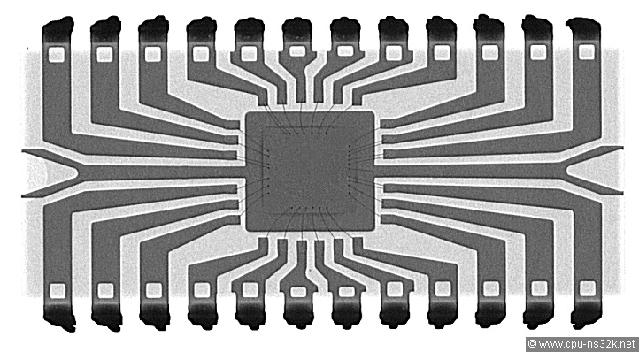
Fig. 35. This X-ray image was made to see where the die is to apply the proper amount of acid. On the right edge of the die the bond wire in the middle is attached to the die carrier to supply the back bias voltage. Pin 1 is in the lower left corner.
![]()
Fig. 36. It is very difficult to identify a chip if only the company logo and a year number is present. Below the year number the "J" may be the design step.
Herbert took a very impressive photo of the die. It has a resolution of 7,250 by 6,720 pixels and the size of the file is 19 MB. I have put the functional names on the used pads.
NS32081 die in very high resolution
NS32381 (FPU)
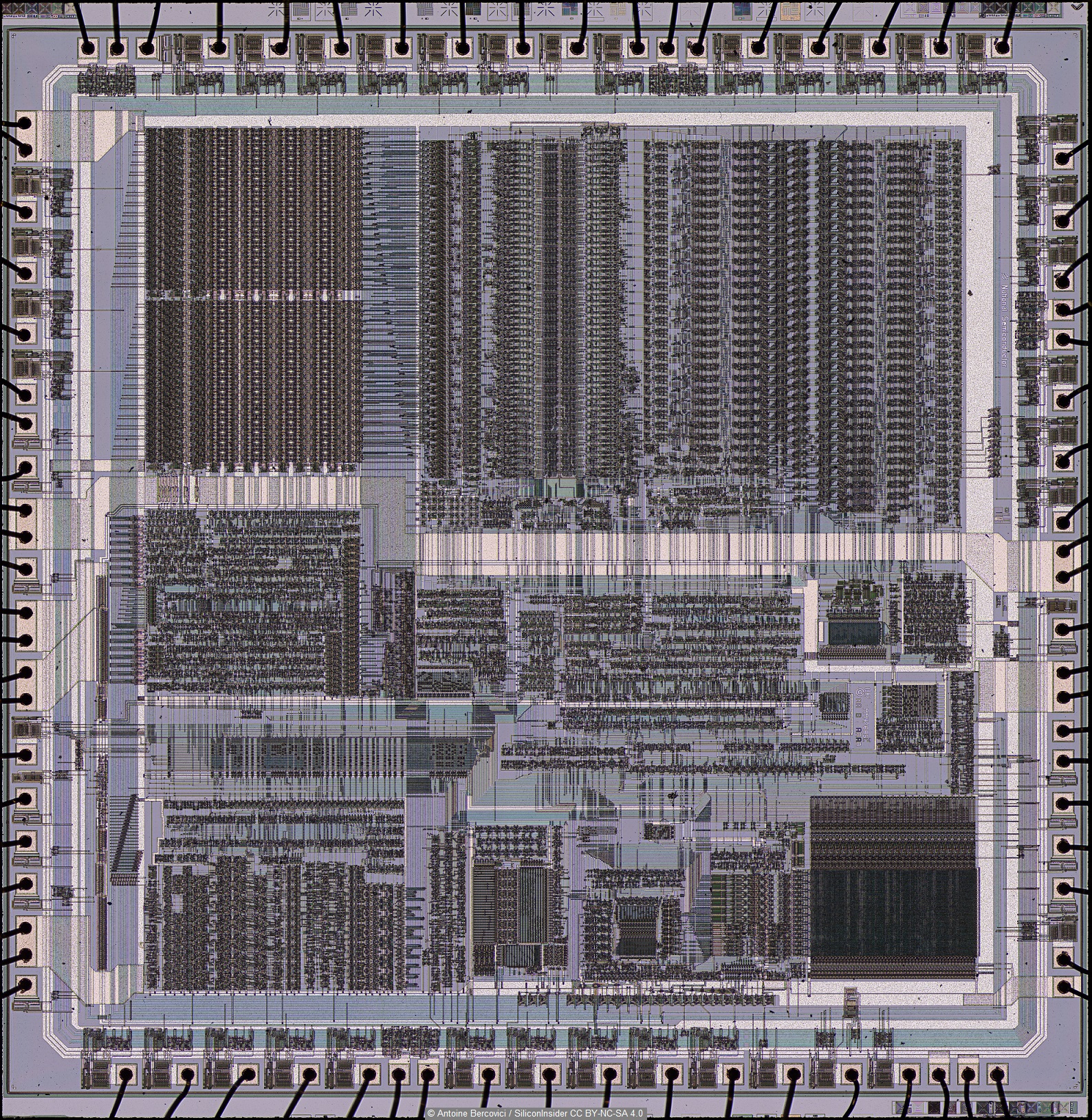
Fig. 37. The second FPU design: the NS32381.
In the upper half you see the datapath of the FPU. A datapath is usual build very regular due to the wide operands. In the left part of the datapath sits the register file (8 by 64 bits). But this is only a guess. The double bonds (two wires on one big pad) at the left and right edge are for power and ground supply. This double bonding helps in reducing the parasitic inductance. There is a date of 1987 on the die near the right edge. Also at the right edge you will find the company name National Semiconductor in full form. Die size is around 8.0 mm * 8.0 mm = 64.0 mm² measured at the outer edge of the pad ring. This is three times bigger than the NS32081 in Figure 32 for only sligthly improved functionality.
NS32580 (FPC)
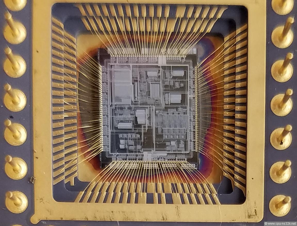
Fig. 38. The one and only floating-point controller: the NS32580. I got the photo from the designer of the chip (Thanks to Shay!).
The NS32580 FPC was designed to connect the Weitek WTL3164 FPU to the NS32532 CPU. Obviously the task did not require that much logic because there is some free space on the die. The black areas contain neither wiring nor transistors. But the design uses many pads and therefore the die is pad-limited. Some area at the upper and lower edges may be dedicated to test logic because it is outside of the pad ring. This is the second device after the NS32CG16 having such large test structures. Maybe first silicon at the end of the 1980's was build on multiple project wafers. Die size is around 7.5 mm * 9.0 mm = 67.5 mm² including the test structures.
NS32082 (MMU)
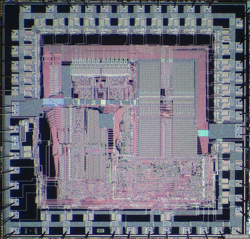
Fig. 39. The first Series 32000 Memory Management Unit: the NS32082. Die size is 6.8 * 6.5 = 44.2 mm². (Birdman86:NS32082)
The functionality of the MMU is not big as can be seen in the die photo of the NS32082. Its main purpose is to translate virtual addresses to physical addresses. This is done by a mapping circuit: the Content Addressable Memory (CAM). It is located in the upper right corner and has 32 entries. The shape of the padring is unusual. The big transistors are located inside the padring. If you compare this layout to the layout of the NS32016 (the transistors are placed between the pads) the conclusion is that the NS32082 is pad-limited.
In 1983 the architecture of the MMU was presented at the ISSCC conference. In the conference paper a die photo is shown. Surprisingly the layout is completely different from Figure 39. Therefore I assume that Figure 39 shows a 2.8 μm version. This explains why the logic core is so small and the die is pad-limited. Of course it would be interesting to find a version built in 3.5 μm technology.
Except for the NS32016 CPU the first generation of Series 32000 was shrunk from 3.5 μm to 2.8 μm. I believe that this was done also for the NS32016. But I have no evidence. Maybe a newer device in a plastic package contains a smaller die (see Figure 4 at Chips/CPUs). I have to ask John for a part ...
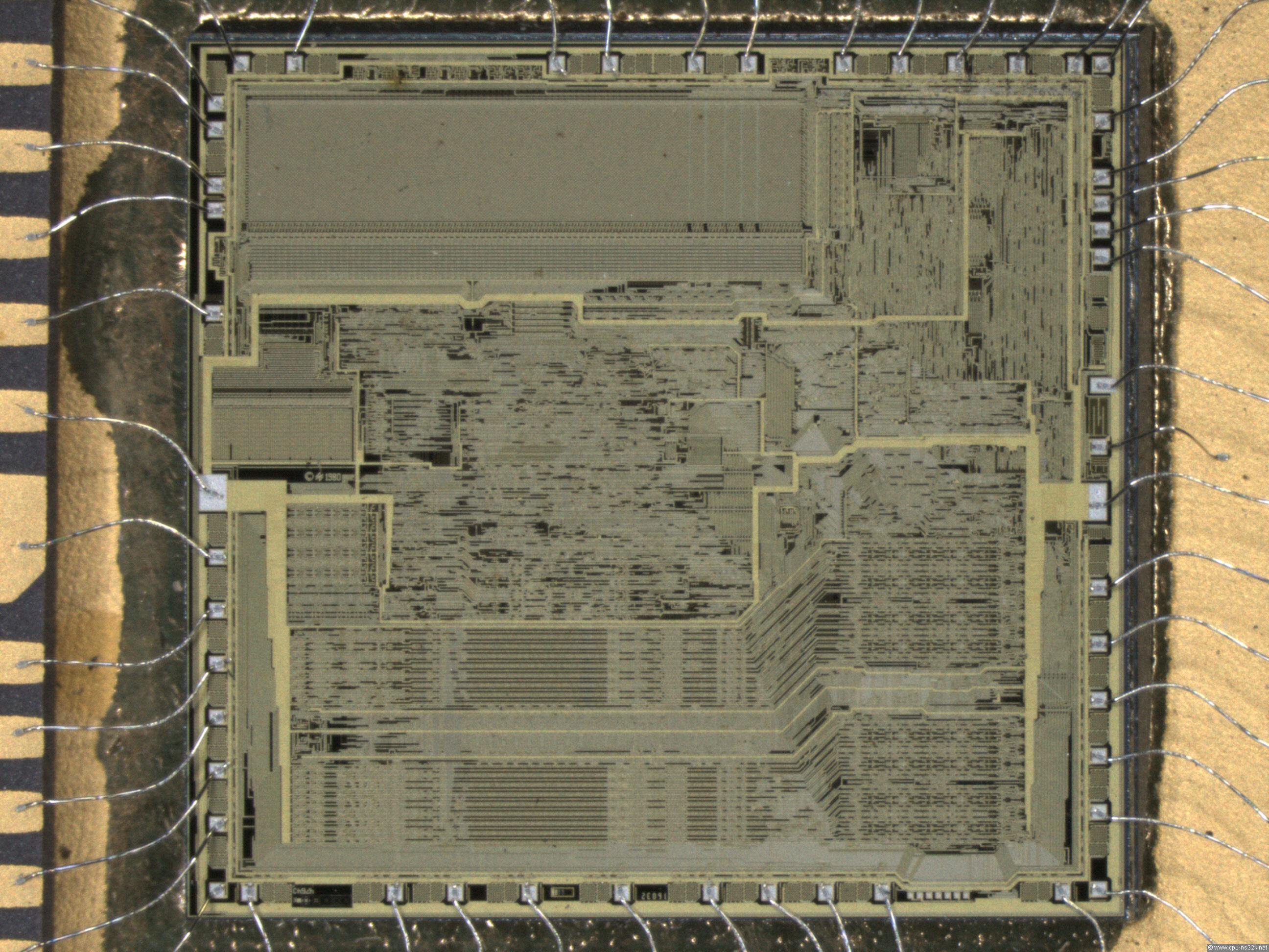
NS32382 (MMU)
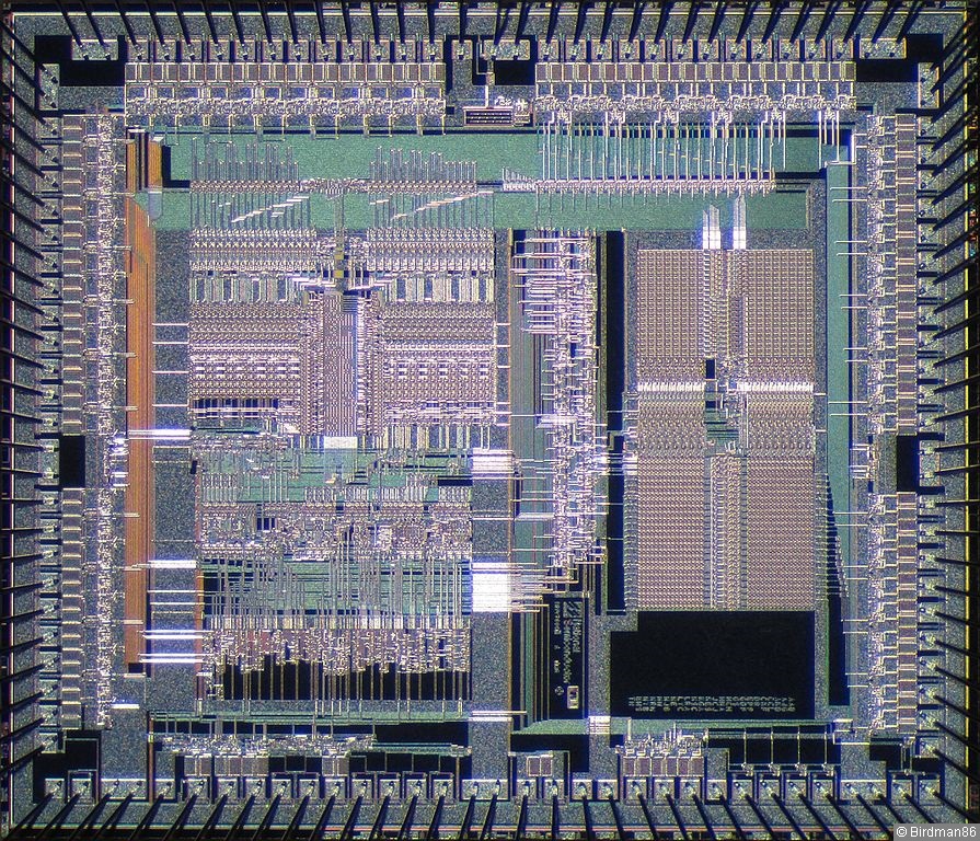
Fig. 40. The second generation Series 32000 Memory Management Unit: the NS32382. Die size is 6.5 * 5.6 = 36.4 mm². (Birdman86:NS32382)
What was said about the NS32082 MMU is perfectly true for the NS32382 MMU: the die is pad-limited. The pads are placed at the minimum physical distance. The number of pins has grown significantly from the first generation to the second generation: from 48 to 125. The reasons are the wider data bus of 32 bits and a new physical address bus of 32 bits. It would be a perfect device if the MMU could have been integrated in the NS32332 CPU. But the 2.8 μm NMOS technology did not allow this.
NS32201 (TCU)
Fig. 41. The Series 32000 Timing Control Unit: the NS32201. Die size is 4.0 * 4.5 = 18.0 mm².
The photo in Figure 41 was taken by a scanner. This was the first time that I used this tool for chip photos. A larger version of Figure 41 is shown in Figure 42. The quality of the photo was a surprise to me.
Fig. 42. A closer look at the TCU showing the bond wires.
National Semiconductor knows the problem of wire inductance. Three bond wires are used for VCC (left) and GND (right). The PHI1 and PHI2 pads have two bond wires each. This pads deliver the two clock phases for the CPU and the MMU.
The cavity of the package is connected by three single bond wires to GND.
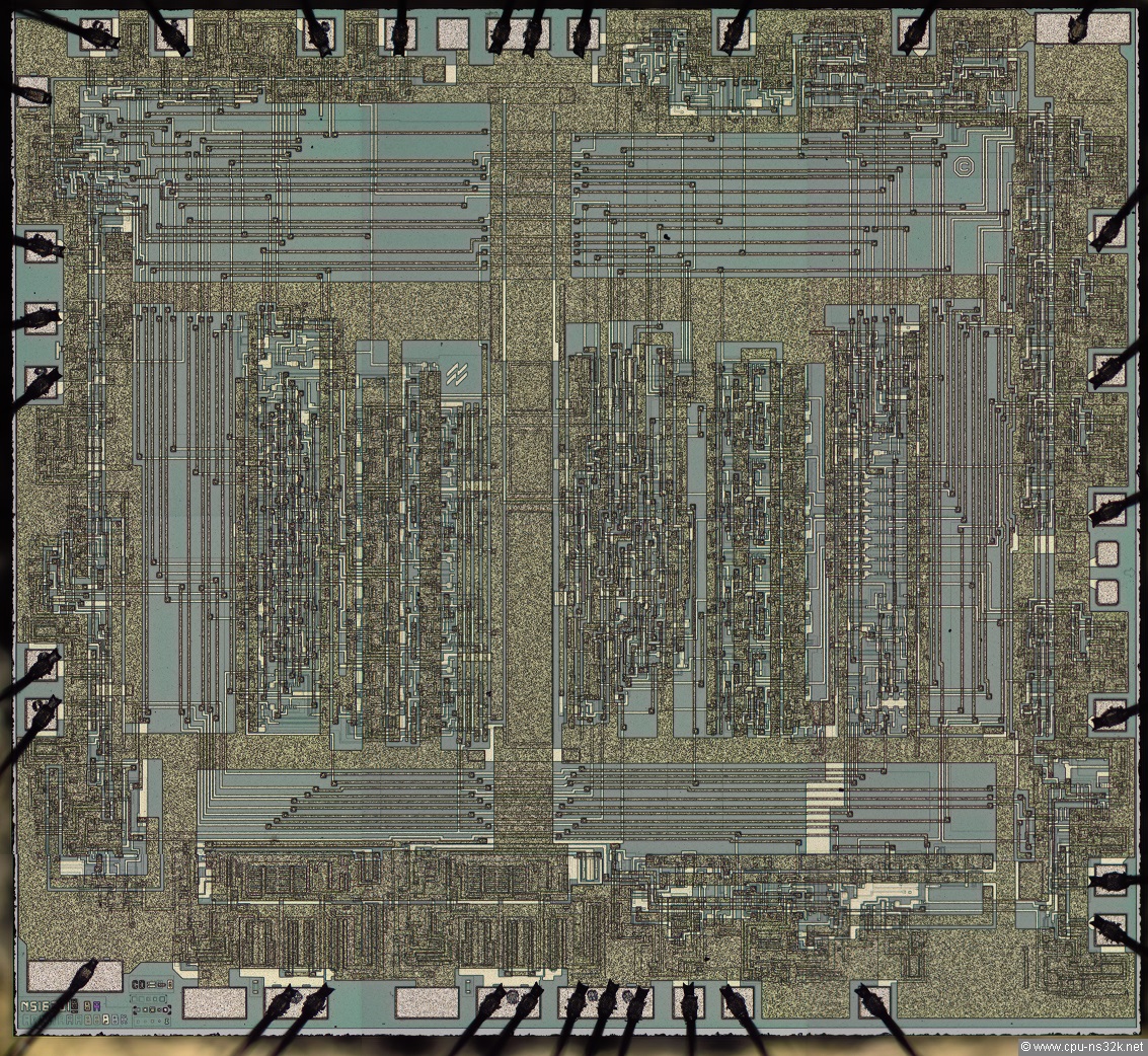
Fig. 43. The die of the TCU. The die is still named NS16201 which can be seen in the lower left corner.
The die is surprisingly big. I had expected a die size of around 10 mm². Obviously much space is used for wiring. Another expectation was to see big buffers/transistors for the clocks PHI1 and PHI2 at the lower left edge. Again a mistake.
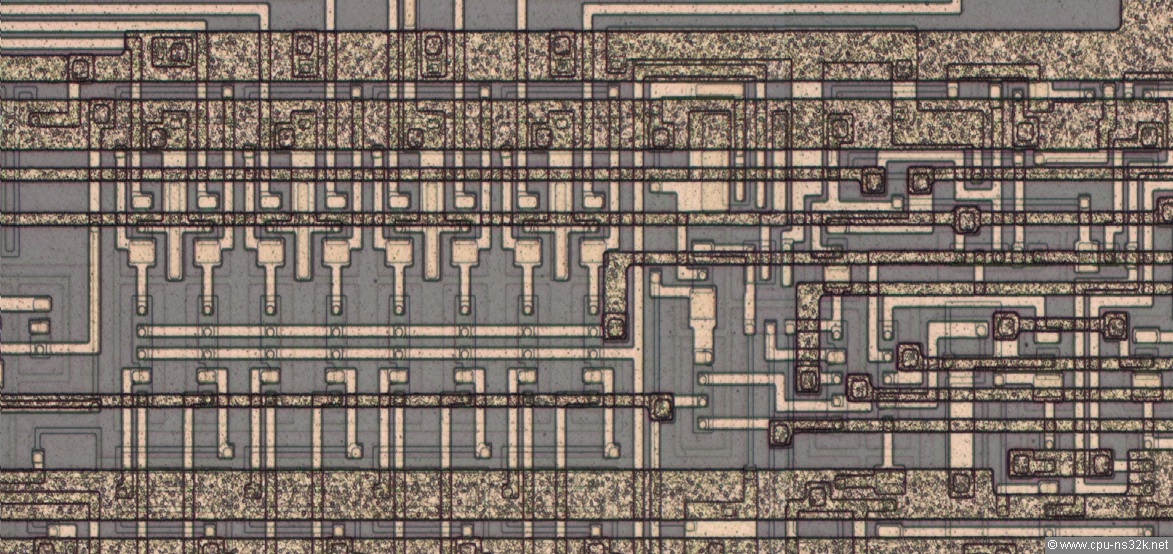
Fig. 44. A detail of the TCU die. I have no idea what it shows...
The NS16201/NS32201 TCU was the only device in the Series 32000 which used bipolar technology. Maybe only this technology was capable in the beginning of the 1980's to deliver sharp edges for clock signals.
NS32C201 (TCU)
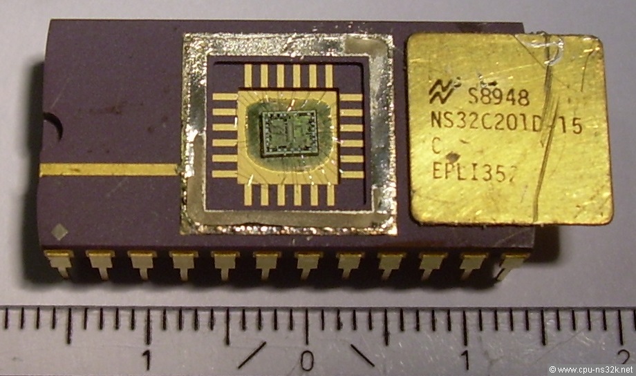
Fig. 45. The NS32C201 is the CMOS version of the NS32201. The die size is only 3.5 * 3.0 = 10.5 mm² which is the smallest of all Series 32000 devices.
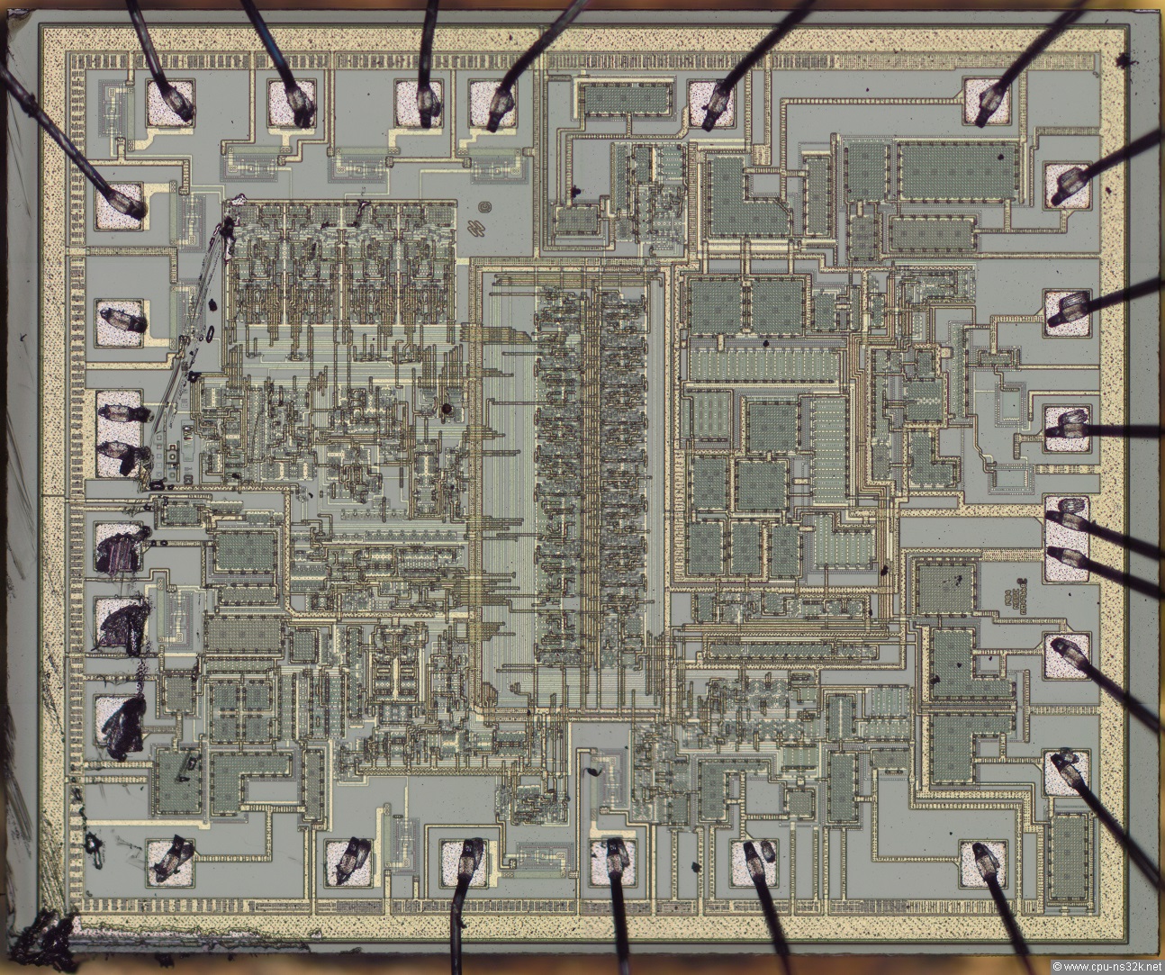
Fig. 46. The layout of the NS32C201 is in my view not nice. Some damage on the left side occured during the opening of the package.
The NS32C201 TCU used much less power than its bipolar predecessor. The highest operating frequency was 15 MHz to support the NS32332 CPU. The NS32201 achieved only 10 MHz.
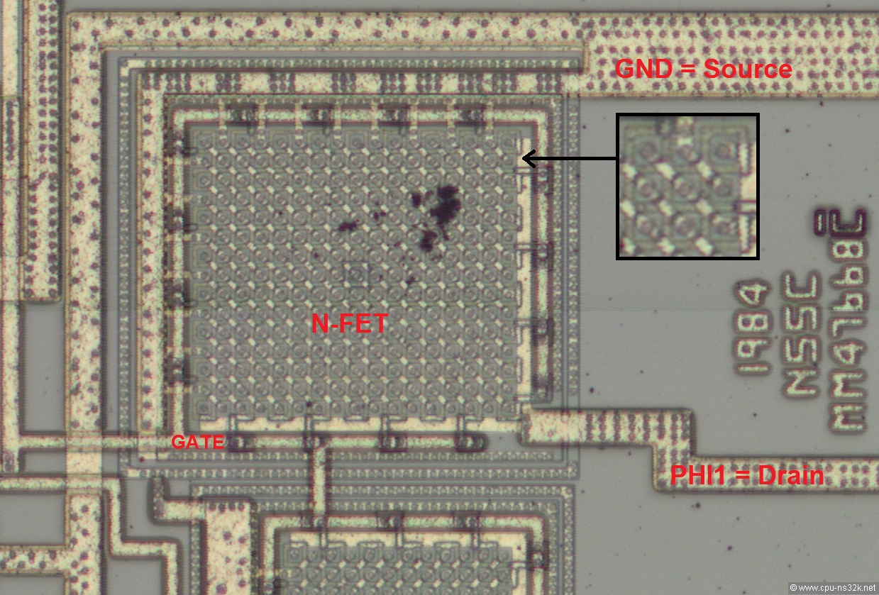
Fig. 47. The layout of the power MOSFETs is interesting: the drain and source contacts are arranged in a chess board style. Therefore the gate length becomes very long. The companies which I worked for never used such a design.
NS32202 (ICU)
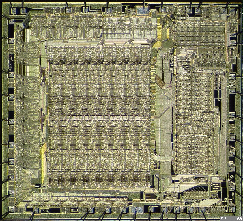
Fig. 48. The Series 32000 Interrupt Control Unit: the NS32202. Die size is 6.4 * 5.9 = 37.76 mm². (Birdman86:NS32202)
One of the simple companion chips of the Series 32000 microprocessors was the NS32202 ICU. It provided a mechanism to control multiple interrupt sources in a system. Although it was a small die National Semiconductor took a lot of money for it, see Miscellaneous/Prices. Later the customers replaced the ICU by their own designs. For example my NS32532 systems use programmable logic devices for this function.
NS32203 (DMAC)
Fig. 49. The Series 32000 Direct Memory Access Unit: the NS32203. Die size is 6.0 * 5.9 = 35.4 mm². (Birdman86:NS32203)
The NS32203 DMAC is a complex chip. It supports four channels. They are identical and can be found in the right half of the die placed from top to bottom. The DMAC supports 24 bit addresses. Therefore it was an useful device only for the first generation of Series 32000 microprocessors.
In the lower left corner seven small testpads are placed inside the padring. This is an unusual location for testpads.
The die of this complex device is surprisingly small. Together with the late date code S9252AB it must being built in 2.8 μm NMOS technology.
Probe Card
I suppose that not everybody has seen a probe card. In germany such a thing is called "needle card". It is used for testing chips which are still on the wafer. This is the first production test and each chip which does not pass this test will not be packaged. Packages could be expensive, for example the 175 pin PGA of the NS32532. Figure 50 and 51 show a probe card of the year 2001. But the concept has not changed since many years.
Fig. 50. The front side of a probe card.
Figure 50 shows a massive metal ring around the probe card. The ring is needed for mechanical stability. During a wafer test the wafer is moved from die to die and the probe card is fixed. Each design has its own probe card.
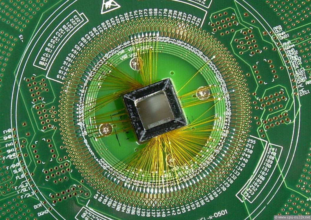
Fig. 51. The back side of a probe card.
If you can't see a single needle - don't worry. In a typical design 10 needles are placed in 1 mm!
This chapter was last modified on 16 September 2023. Next chapter: Systems/Acorn