Project C7
In 2018 I noticed that my Cyclone V GX Starter Kit from Terasic has a nice feature. It is possible to upgrade the FPGA to a bigger member of the Cyclone V GX device family. The board is sold with the 5CGXFC5C6F27C7 device. I call it the "C5" device. It contains 29,080 ALMs (ALM=Adaptive Logic Module), 446 memory blocks of 10kbit each and has 6 transceivers. 4 of them can be used on the Starter Kit.
The next bigger device in the family is the 5CGXFC7D6F27C7. I say "C7". It has 56,480 ALMs, 686 memory blocks and 9 transceivers. There is an even bigger device available with more than 100,000 ALMs. But in my feeling it is too big. Such a device should be a member of the high performance family of STRATIX FPGAs from Intel/Altera. Of course the price is higher for bigger devices.
The next Figure shows the original FPGA of the Starter Kit.
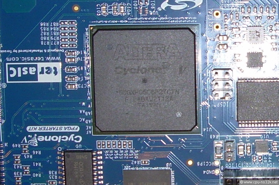
Fig. 1. The "C5" of the starter kit had a colored label on it. The reason is that the plastic package looks not very impressive. I took the label off for the desoldering process.
It took 5 years until I could realize the exchange. In 2020 we got the Corona crisis and in 2021/22 we got the semiconductor crisis. It was not possible to get any FPGA. In 2022 the distributors wrote that my device will be available in 2024. But in Summer 2023 two devices were offered at DigiKey. I bought one of it. It was more expensive than the Starter Kit...
Now comes the difficult part. Who will do the exchange? For me it is impossible. I have not the equipment and misses the experience. But I know a small one person company who does soldering work. The person said "No problem, I'll do it" and the next Figure shows the result. I have not seen any smallest damage either on top of the board or on the bottom side (I took off the three pins of JP14 to get more space for the desoldering tool). Impressive!
But despite that all looks good I was very nervous when I first applied power to the board. And I did many stupid mistakes until I was sure that the exchange was successful.
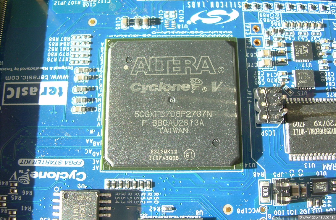
Fig. 2. This photo is taken in bright sunshine and now the text on the "C7" is easily readable. Please note that nothing has happened to the surrounding parts.
The actual current delivered by each voltage generator on the Starter Kit can be measured. The internal logic of the FPGA uses 1.1 V. The "C7" needs at the moment a current of 540mA. The generator can deliver 5A. Therefore the logic can become much more power hungry. I planned to use a heat sink for the FPGA. But I will put on one only if the current gets above 1A. The 672 balls of the FBGA package transfers the heat very well into the pcb.
Chip Planner
A nice feature of the Quartus development software is the Chip Planner. It shows the struture of the chip and the placement of all elements of a design. The next Figure shows the "C5" containing the TRIPUTER V2.0.
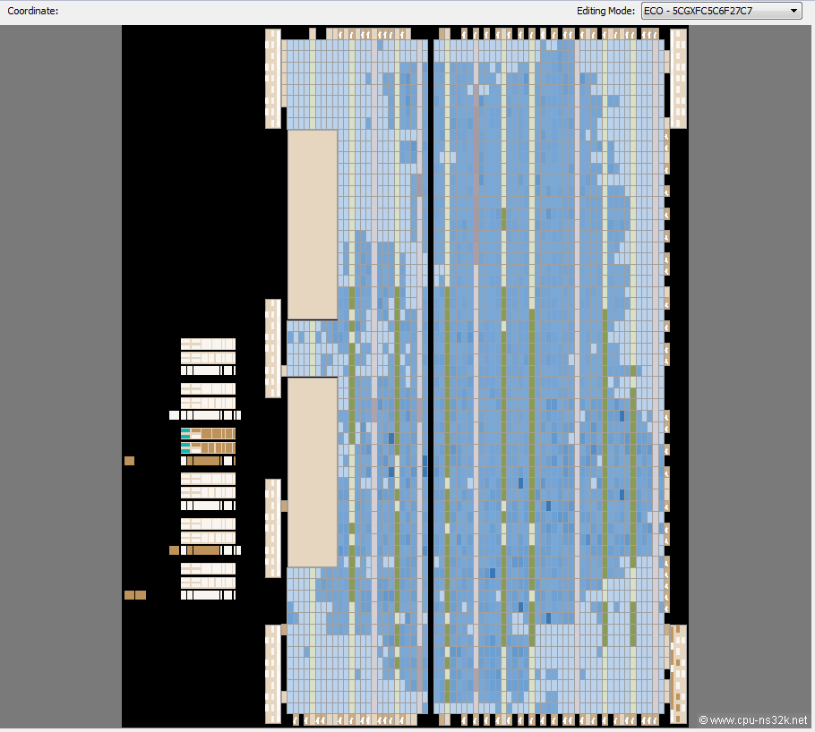
Fig. 3. The Chip Planner shows where all elements of TRIPUTER V2.0 in "C5" are placed.
Each blue rectangle is a Logic Array Block (=LAB). It contains 10 ALMs together with very short interconnects. In addition the block has some common control signals, for example clocks and resets. The LAB is connected to the general routing. The intensity of the blue color indicates the usage of the LAB. Light blue says the LAB is not used. Dark blue says the LAB is 100% used. In the above picture the number of fully used LABs is very low. The compiler has no problem to place the 13,410 ALMs of TRIPUTER V2.0.
"C5" has 2908 LABs (You want to count them?). Around half of the LABs can be used as small SRAMs. The 10kbit SRAMs are placed in the green stripes. Again if it is light green the SRAM is not used. The red stripes are the place for the DSP block. A DSP block is mainly a configurable multiplier of 27 by 27 bit. TRIPUTER uses only a few of them, for example in the floating point multiplier.
What are the two light brown areas I don't know. On the left inside the black area the 6 transceivers of "C5" are placed. One of them is used for the SATA interface.
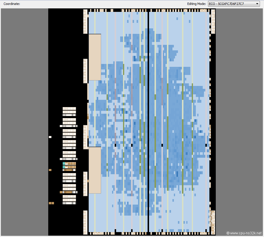
Fig. 4. The Chip Planner view of "C7" can't show the boarder of each rectangle. The chip is simply too big. Of course you can zoom in.
The "C7" has much more ressources compared to "C5", see the Figure above. The design needs at the moment 19,127 ALMs. Of the 9 transceivers on the left only one is used.
Next chapter: TSMC 16nm FinFET